Hello, I’m Steven Mill and today I want to write about Nanoscale energy efficient switching devices.
Saving energy is becoming one of the top priorities of scientists across the globe and extensive research is being carried out to introduce cutting-edge techniques that will help in conserving as much energy as possible.
In this regard, researchers have been working on inventing nanoscale switching devices that are supposedly highly energy efficient and very robust in terms of structure and function.
Introduction to Nanoelectromechanical Switches
Nanoscale switches or commonly known as nanoelectromechanical switching devices are a very important step towards revolution in the electronics industry. Made up of silicon carbide, the switches are about one cubic micron in volume. The small size suggests that we will be able to incorporate trillions of these devices in a computer chip or circuitry. The best thing about NEMs is their exquisite performance. They can operate at more than a billion cycles in air which is greater than any switching device known to man. Their durability can be noticed by the fact that they can operate at about 500°c or 930°F, which is double the temperature a conventional silicon based switch can endure.
Although, silicon-based MOSFE transistor is considered as the core of electronics industry and is heavily utilized in computers, tablets and androids, but despite its effectiveness, it isn’t much of an “energy saver.” Energy is lost in the form of heat because electrons travel across the switch even if it is off. An estimate shows that the power losses in a typical MOSFET are about 5-10 nanowatts and with trillions of MOSFETS in a computer chip or extensive circuitry, these losses can accumulate up to tens of watts. But, in case of NEMS devices, energy losses are too minute to be noticed.
Another great aspect of developing nanoelectromechanical switching devices is that they are immune from oxidation, chemical contamination or wear and tear with time which makes them perfect to be produced in bulk at a very reasonable cost.
Application of NEMS Devices
Nanoelectromechanical switches have great applications in a number of fields that are being explored nowadays. NEMS are used in sensing devices, portable power generation, displays, drug delivery, and imaging etc.
Nanoelectromechanical Sensors
Development of nanoelectromechanical sensors is a major achievement in our journey towards miniaturizing machines and electrical devices. A few years back, microscale sensors were the peak technology used, but now, due to the successful innovation of nanoscale sensors, others will soon be wiped out. This is because the NEMS sensors are a thousand times better and they have a greater number of applications than microscale sensors.
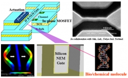
NEMS sensors involve a variety of sensing categories. The first one is the physical sensors used to detect changes in rotation, acceleration, pressure, temperature, velocity, etc. These sensors are based on the principles of mechanical displacement to expansion, and atomic spin alignment.
The second category of sensors is chemical sensors used in chromatography, resonance studies and mass spectrometry. Similarly, the nanoscale bio-sensors have great applications in measuring blood sugar level, identifying diseases, DNA analysis and electrophoresis. After bio-sensors come nanomechanical signal sensors. These sensors are very novel and are widely used in computation, frequency generation, amplification, logic gates, A/D convertors, memory and antennas.
Last but not least, the optical sensors. These are required in the formation of chip-scale atomic clocks, optical tables, lasers, photodetectors and spectroscopic sensors to identify nanoscale substances.

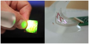
Nanoelectromechanical Systems in Display Devices
The markets are full of display devices like monitors, LCDs, LEDs, Plasma screens and android and tablet screens. The best screens among these are of Plasma T.V sets and android and tablet screens. They demonstrate great display but are very expensive. In order to replace these devices, successful research is conducted to produce nanoscale materials that won’t be much expensive and will also show far better display than plasma or tablet screens.
One of these materials is commonly known as GNEMS or graphene based nanoelectromechanical switches. Graphene is a brilliant conductor made up of graphite that can conduct at a much faster rate and is less expensive than indium tin oxide used in plasma TV screens.
Drug Delivery via NEMS Devices
MEMS based drug transfer materials are now becoming commercially feasible because of their low production costs and ease in using these devices. Combination devices created using NEMS technology have the tendency to meet a number of medical requirements associated with dosing. These products can easily regulate drug release and meet the needs for changeable continuous supervision for prolonged periods.

If Nanoscale biosensors and drug storage units are joined and installed, a wireless unified system can adjust drug release, receive feedback from the sensor and then spread updates. The examples of such phenomenon include the installment of artificial pancreas and nanosensors attached with it that help in monitoring diabetes.
Conclusion
Nanoelectromechanical systems are the dawn of development in electrical and electronics industry. These systems are better in every way than the primitive one, but research is still being conducted to improve these systems in order to make them close to perfect.
What do you think about these switching devices? Did you know about them?