Home › Electrical Engineering Forum › General Discussion › Improving Light Absorption in Semiconductors through Optical Nanoactivity
- This topic has 1 reply, 2 voices, and was last updated 11 years, 8 months ago by
 Anonymous.
- AuthorPosts
- 2014/06/03 at 4:04 pm #11169
 adminKeymaster
Hi, this is Steven Mill and as you may have noticed, I crazy about electricity and its application to our modern world. Once again I want to tell you about the evolution of the techniques and the improvement of electrical devices through an article. Feel free to approve or not my explanation below…
Physicists and researchers across the globe have indulged themselves in conducting researches that are of extensive benefit to mankind. With each progressing year, considerable developments are made in different domains of physics that make use of cutting-edge science in order to facilitate human course of existence as much as possible.
Over the recent time, extensive focus has been given to the study of light phenomenon in such a way that maximum light absorption is made possible in semi-conductors. Optical Nano activity has played a great role in this regard.
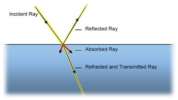
What is really meant by light absorption?
In physics, light absorption refers to the transference of energy of the wave as it passes through any particular material. It must be kept in mind that light absorption is a diverse phenomenon and varies from substance to substance.
Reflection, absorption and partial diffusion are all properties of light. Normally, it is stated that black surfaces tend to absorb all light which likely explains why all black stuff may appear very hot.

Keeping in view the above illustrated 3 qualities of light, physicist base optical considerations for surfaces that can be deemed best for light absorption.
Semiconductors
Semiconductors are those material which possess dual properties. Their conductive properties are similar to those of good conductors such as copper but at the same time may have excellent insulation qualities such as those possessed by glass.
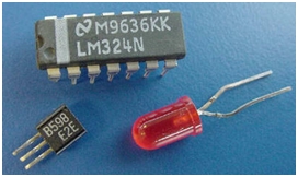
Semiconductors can be called as the heart of machinery that we use every day as they include transistors, microprocessors, diodes, LED’s etc.

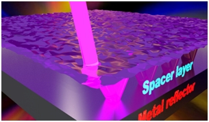
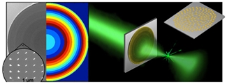
Optical Nano-cavity
Optical Nano cavity is obtained by arranging slot of mirrors in such a way that beams of light circulate with in closed paths. Through the development of optical Nano-cavities, avenues for abundant development in physics domain have opened up.

How has light absorption in semi-conductors improved through the use of Nano cavity?
Electrical engineers have developed such semiconductors that have an enhanced tendency of absorbing light much more than ordinary surfaces. As stated in the Journal of Advanced Materials, silicon is the most commonly used semiconductors of all. But the major problem associated with the use of ultra-thin semiconductors is that their light absorbing competency is much less, as a result of which their electricity generation ability is highly affected.
In this regard, many successful attempts have been made to improvise the existing structure of semiconductors. Scientists have brought into use germanium plated on gold surface to obtain valuable results. However, what needs to be kept in mind is the expensive nature of gold metal.
Therefore, researchers have begun conducting experiments not just with aluminum but other alloys as well. They are not just cheap but would exceedingly enhance the light absorption by semiconductors. Owing to the hard work of many researchers, such Nano cavity has been made that comprises of a combination of aluminum, aluminum oxide and germanium. This cavity has rendered remarkable results to the fraternity and proposals for carrying out further tests are underway.

Applications of semi-conductors with improved light absorption
With semi-conductors being improved to a great extent and having incredible light absorptions quality, list for its wide ranging applications becomes endless. Some of the basic and fruitful implications of semiconductors that have been strengthened through the use of Nano cavity are stated below.
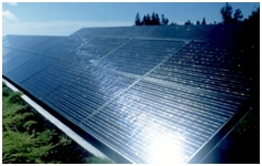
- Photovoltaic cells: An improved light absorption definitely means development of such photovoltaic cells that are structured in the best possible way to capture light. In this way, not just light energy would be brought in use but the burden resting on the shoulders of electrical energy would be slightly relived as well. The energy harvesting solar cells surely play the best part in conserving and utilizing the solar efficiency.
- Improved video cameras: Researchers aim in the enhancement of Nano cavity technology in such a way that an ultra-thin optical film absorber is devised. This would lead to improved video cameras and making it all the way more quick and meaningful to capture most memorable events of life.
Precision, quality and agility to video camera is all due to enhance light absorption by the semiconductors. At the same time, better and efficient security system could be achieved by developing such security cameras that absorb light at a much faster pace than conventional cameras. - Nano-optical Antennas: Another perk associated with the development of well-developed semi-conductors, is the Nano-optical antenna. This works dramatically different to the conventional signal catching devices in use. Use of light coupled with signals strongly improve the quality and speed of signal detection as well as transmission.


Conclusion
Light absorption has considerably improved by improvising the conventional semiconductors through the aid of Nano-cavities. It would be totally justified to claim that researchers and electrical engineers have taken bold and productive steps in studying the phenomenon of light in such a way that it yields best results for mankind.
Steven Mill.
2014/09/11 at 9:29 am #13560AnonymousGuestGood day I am so happy I found your web site, I really found you by accident, while I
was looking on Yahoo for something else, Anyways I am here now and would just like to say thanks a lot
for a incredible post and a all round thrilling blog (I also love the theme/design), I don’t have time to read through it all at the
minute but I have saved it and also added your RSS feeds,
so when I have time I will be back to read much more,
Please do keep up the awesome jo. - AuthorPosts

- You must be logged in to reply to this topic.