Home › Electrical Engineering Forum › General Discussion › A practical switch power produced (schematic diagram + PCB)
- This topic has 1 reply, 2 voices, and was last updated 11 years, 7 months ago by
 davejo.
- AuthorPosts
- 2013/08/30 at 4:23 am #11074
 AnonymousGuest
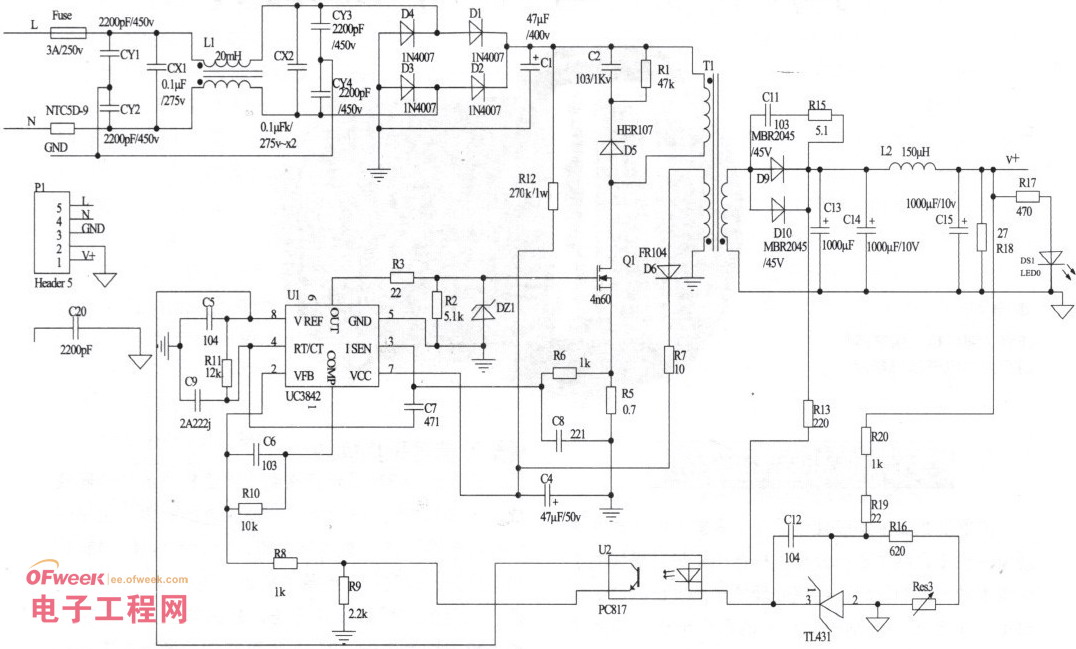
Anti-jamming circuit.
USES the ceramics with good high frequency characteristics of capacitance and iron core inductor, switch regulated power supply circuit to realize the high frequency radiation pollution power frequency not stray on the grid and grid power frequency electromagnetic wave not into a switching power supply circuit and interference and influence its work, the high frequency component or power frequency harmonic component has a sharp stop by function, and for a few hundred hz low frequency component of the approximation under a shorter route.
2. The rectifier filter circuit
D1, D2, D3, D4 in the circuit of the whole bridge rectifier circuit, the input ac voltage of full-wave rectifier, and then use C1 for filter, and finally into a dc output voltage, a category after power inverter power supply, the voltage of the rectifier filter after about 300 v.
3. The power supply and UC3842 oscillations
Pulsating dc voltage 300 v, the voltage after R12 step-down to C4, charging power supply of UC3842 7 feet, when the voltage of C4 reaches UC3842 start-up voltage threshold value, the UC3842 began to work, and provides the drive pulse output from 6 foot switch tube. Once the switch tube, the energy feedback winding through the D6 rectifier, C4 filter, and the power supply to the UC3842 7 feet, can not at this moment need R12 started.
C9, R11 UC3842 timing, and the internal circuit oscillation circuit, the work frequency of the oscillation calculated as:
F = 1.8 / * Ct (Rt)
Generation into the working frequency of data can be calculated:
F = 68.18 K
4. The voltage regulator circuit
This circuit mainly by the precision voltage source T L 4 3 1 and linear light coupling P C 8 1 7, assuming that the output voltage and write 1 9 after 1 6 R, R, the R20, RES3 and write the sampling voltage TL431 voltage write 1 foot, when the voltage is greater than the TL431 feet when the reference voltage of 2.5 V, the TL431 conduction, 2, 3 feet – through photoelectric coupling to 2 feet of UC3842, and UC3842 6 foot drive pulse duty ratio left to switch on the T1 transformer energy left, left the output voltage, voltage stabilizing role; On the contrary, assume that the output voltage drops, is contrary to the regulated process.
R9 UC3842 obtain feedback voltage input, the R8 and R10, C6 is to change the UC3842 internal gain and frequency characteristic.
5. Over-current, over-voltage, under-voltage protection circuit
Due to the input voltage is not stable, or some other external factors, sometimes prompted a short circuit, overvoltage, undervoltage circuit phenomenon unfavorable to the circuit work, therefore, the circuit must have a certain protective function.
(1) the over-current protection. If for some reason, output short circuit and over current transformer winding to switch the quick release of energy, in order to replenish the energy, the switch tube must be extended drain current of the conduction time to switch tube to rise sharply, R5 on both ends of the voltage rise, voltage on UC3842 foot 3 and up. When the feet of the voltage more than normal 1 V, 0.3 V to the inside of the UC3842 PWM comparator output high level, to reset the PWM latch, close the output. UC3842 feet 6 no output, switch tube cut-off, over-current protection.
(2) overvoltage protection. If the power supply voltage over-voltage (above 260 v), will greatly improve the transformer primary winding voltage sampling on the winding voltage after rectifying filtering makes UC3842 feet 7 voltage also rose sharply, its feet 2 voltage rise, also shut down output, 6 foot switch tube stop, over voltage protection.
(3) the under-voltage protection. If the grid voltage is lower than 90 v, the foot of UC3842 1 voltage drop, when below lV, the inside of the UC3842 PWM comparator output high level, to reset the PWM latch, close the output 6 feet. Realize the under-voltage protection.
6. The output rectifier filter circuit
D9, D10, C13, C14, C15 is the output rectifier filter circuit, this part of the circuit part of high frequency filter.
D9, D10 for schottky diode, the high frequency fast recovery of switching diode characteristics, and has low positive tube voltage, fast switching speed, as the reverse leakage current is small, will help improve the efficiency of power supply, the reverse recovery time is short, is helpful to reduce the high frequency noise.2014/09/25 at 4:47 pm #13605davejoParticipantcici, this is an excellent design and it the way you have documented all the related issues is excellent. I need a small anti-jamming circuit for my GSM circuit and I was wondering how I can tune this particular circuit. From the looks of it, it stop the high frequency components and the low frequency components from a signal. It’s not very difficult to understand but what if I want to tune it in order to remove noise from the similar frequency that I’m tuned to listen the signal on.
- AuthorPosts
- You must be logged in to reply to this topic.