 We’re happy to publish this new article by Mile, your fellow electrical engineer who has kindly been sending us articles for several months now.
If you want to, you can do like him and send us an email. We’ll be happy to publish your essay!
Introduction
The conversion of electrical power from ac to dc, whilst maintaining sinusoidal input currents at unity power factor, is widely achieved using a variety of power converters.
Many applications make use of the boost converter due to the simple design and switching control, and its ability to produce a range of dc output voltages larger in magnitude than the output voltage of a standard bridge rectifier, which is desirable in many applications. A buck converter provides a high power factor if only a low dc output voltage is required. This article outlines a new design of a three-phase buck-boost power quality converter.
The function of a buck-boost converter consists of two distinct operations. Firstly, the converter inductors are charged via semiconductor switches from the mains. Secondly, the stored energy discharges to the load providing power transfer, usually through load filtering circuits. The output voltage varies by controlling the switching duty cycle of the semiconductors. Many of the existing three-phase buck-boost topologies require complicated switching methodologies to provide a high power factor, or alternate switching of devices in both the mains supply and dc side of the inductors, requiring snubbing and careful synchronization. The proposed topology requires only simple chopper control, whereby all switches are switched simultaneously.
A new type of three-phase buck-boost power quality converter will be designed specifically as a prototype for a 20kW DC power supply, providing a 300-600V dc output voltage range from a three- phase mains supply (415V).
Configuration and modes of operation
In picture 1, voltage sources V1,V2 and V3 represent the 3-phase power supply. Inductors L1.L2 and L3 and capacitors C1,C2 and C3 form the line filter, while the switching is performed by three IGBTs, Z1,Z2 and Z3, with integral anti-parallel diodes, D1,D2 and D3, providing the return current paths. Inductors L4,L5 and L6 are the high frequency buck-boost energy storage inductors. A load-smoothing filter is included (C4, L7, C5).
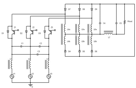
Picture 1. Circuit layout
There are three states during the converters operation:
State 1: Charging of the converter inductors L4,L5 and L6 from the supply via Z1,Z2 and Z3 without energy transfer to the load and filter circuit.
State 2: Energy transfer from the converter inductors to the load circuit while Z1,Z2 and Z3 are non-conducting.
State 3: Charging of the converter inductors with energy transfer to the load circuit.
Operation in the State 1 is presented on picture 2.
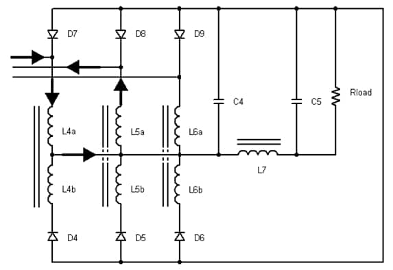
Picture 2. Operation-State 1
If V1 has the largest positive instantaneous magnitude and V2 has the largest negative magnitude, when Z1,Z2 and Z3 are closed, current will build up in the L4 and L5 converter inductors.
In state 1 none of the converter diodes apart from D2 will be conducting and as result the supply energy is stored in inductors L4 and L5.
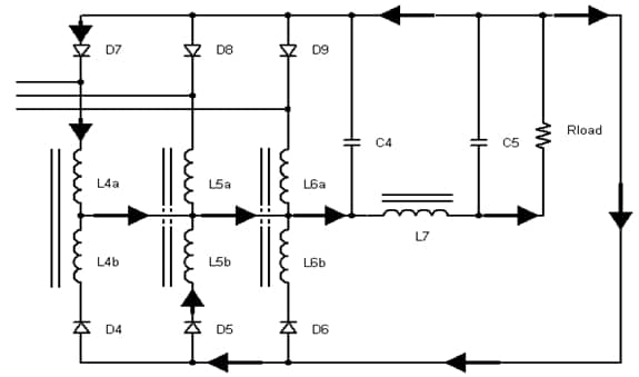
Operation in State 2 is presented on picture 3.
Following the turn off of Z1, Z2 and Z3, the energy stored in inductors L4 and L5 will be transferred to the load via diodes D7 (for L4), D5 (for L5) and the load-smoothing filter, C4, L7 and C5.

Picture 3. Operation-State 2
Operation in State 3 is presented on picture 4.

Picture 4. Operation-State 3
When Z1 is closed, through L4, L5 and D2, current will build up, like in State 1.
If there is no need for energy transfer to the load at all during this period, L7 may be replaced by a fourth IGBT, synchronized to close immediately after Z1,Z2 and Z3 open. This allows the power flow from the inductors to the load and effectively limiting the converter to operate in the State 1 and State 2 only.
Operational characteristics
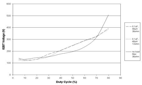
The variation in load voltage as a function of switch duty cycle is shown on picture 5.
The design of the load filter, i.e. C4, L7, C5, can be optimized to produce the desired output voltage for a specific load. The presence of the load filter is significant in maintaining a linear output voltage response as a function of the switching duty.
The value of C4 should be small, because a large value will provide increased reservoir capacitance and a nonlinear output characteristic. Ideally, a low value for C4 will produce a near linear characteristic.
Picture 5. Typical output voltage trends
It can be seen from picture 6 that the peak IGBT voltage depends on the switch duty, and is also affected by the presence of the load filter C4, L7.
Picture 6. Typical IGBT peak voltages
Conclusion
This new type of power converter provides a wide range of DC output voltage at a high-power factor. Operational characteristics, i.e. variation of output load voltage as a function of the input voltage, the duty cycle and the value for the filter capacitor are presented and analyzed. The design optimization of the load filter, to produce the desired output voltage for a specific load is performed. The influence of the load on the output voltage response as a function of a switching duty is discussed.
Thank you all for reading,
Mile.
What do you think of this new type of 3-hease buck-boost power quality converter and what can you say bout it? Comment below toshare your opinion!